Micro-electromechanical systems, or MEMS, may not be on your mind, but there could be some in your pocket.
Your smartphone likely uses a dozen or so tiny — yet powerful — MEMS sensors to support its sophisticated functions. And that late-model car undoubtedly carries scores of devices based on MEMS and other sensing technologies.
Typically sized at the micron scale — millionths of a meter — MEMS devices use minuscule moving parts to perform a broad range of sensing tasks. Small as they are, they can detect sound, motion, position, force, pressure, chemicals, bacteria, and numerous other things worth knowing about. Note that these miniaturized sensors don’t always have moving parts, and a broader term — microsystems — is sometimes used rather than MEMS.
At Georgia Tech, more than 20 research teams focus on MEMS-related research and development. Supporting them is the Institute for Electronics and Nanotechnology (IEN), one of Georgia Tech’s nine Interdisciplinary Research Institutes. IEN’s extensive shared-user facilities, including advanced labs and cleanrooms, are used by as many as 200 Georgia Tech faculty, graduate students, and postdoctoral researchers who work on MEMS and other microsystems.
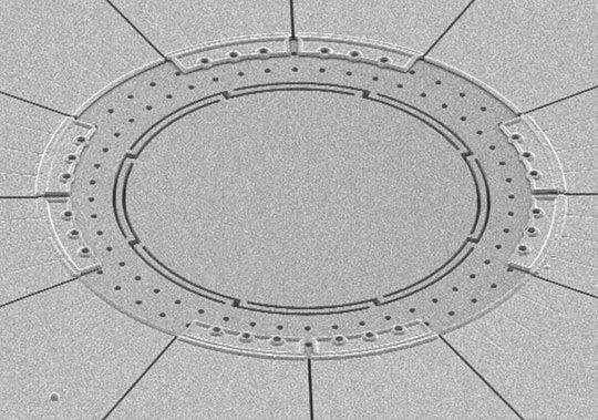
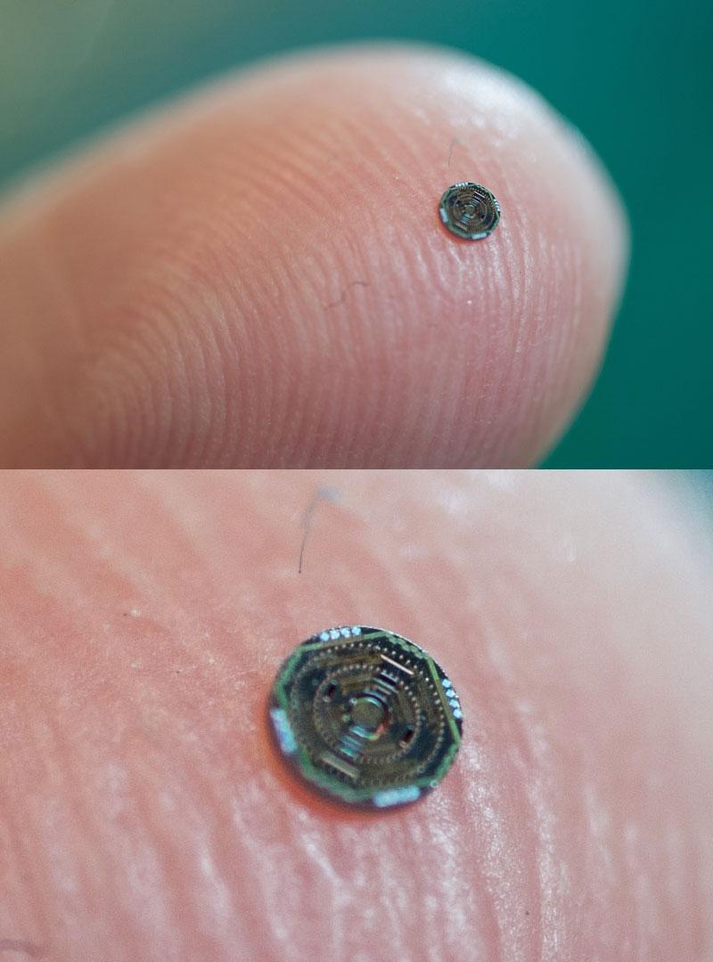
This annulus resonator gyroscope, designed in Farrokh Ayazi’s laboratory and fabricated in Georgia Tech cleanroom facilities, is a mere 800 microns across yet measures rotation around two in-plane axes — pitch and roll. A similar design being developed measures rotation around all three axes — yaw, pitch, and roll — using a single tiny device.
“More and more, our electronic systems must be aware of and even interact with their environment, and MEMS-based devices do that very well. They are the ear that detects sound and movement, the nose and tongue that detect toxic chemicals or smoke,” said Oliver Brand, a professor in Georgia Tech’s School of Electrical and Computer Engineering and executive director of IEN. “MEMS is like a sandbox of technologies and processes that lets us miniaturize sensors, and even put several sensing technologies onto a single chip, at low cost. It can enable many innovative applications, and it can also make conventional devices — like smoke or movement detectors — smaller, smarter, and more effective.”
Creating innovative sensors is highly interdisciplinary, Brand noted, requiring the joint efforts of electrical engineers, mechanical engineers, chemists, and biochemists — who are, in turn, supported by materials, packaging, and circuit-design experts. In addition, MEMS development is often expensive, demanding advanced facilities with device fabrication and characterization tools.
IEN enables Georgia Tech researchers to address these challenges, Brand said. Its cleanrooms and associated labs, open to Georgia Tech and non-Georgia Tech researchers, make state-of-the-art fabrication and characterization equipment widely available. As a result, most MEMS prototypes under development at Georgia Tech can be built right on campus.
Many of these micron-size devices utilize even smaller elements — nanotubes and nanowires — that aren’t much larger than a single molecule. These tiny nanoscale parts help microsystems detect what they’re looking for. The presence of moving nanoscale elements has given rise to the term nano-electromechanical systems (NEMS), but most researchers just use the term MEMS.
A wide variety of MEMS-related and microsystems projects are underway at Georgia Tech. The following is a sample of current MEMS research in the fields of consumer products, health care applications, environmental sensing, and infrastructure monitoring.
MEASURING MOTION AT THE MICROSCALE
In the Integrated MEMS Laboratory at Georgia Tech, Professor Farrokh Ayazi and his research team are working on groundbreaking techniques for accurate motion sensing. In particular, they’re focused on very small gyroscopes, which detect rotation and are integrated on a silicon chip along with precision low-power accelerometers, which measure linear motion.
Ayazi’s research into MEMS-based devices has produced inertial measurement microsystems with applications in automotive, navigation, robotics, gaming, and more. These devices could help both conventional and driverless cars navigate safely, or they could track the location of a person or other moving object in situations where GPS signals are problematic or absent.
“Think of MEMS-based microsystems as multi-domain, with complex mechanical, fluidic, or optical devices working in tandem with electrical devices, all integrated and packaged together on a common tiny substrate,” said Ayazi, a professor in Georgia Tech’s School of Electrical and Computer Engineering.
Professor Farrokh Ayazi has developed tiny gyroscopes that use MEMS technology to track firefighters or other first responders in covered areas where GPS signals are stymied. Here, he tests the technology at the Krog Street Tunnel, an Atlanta landmark decorated by local artists.
Front-end micromechanical sensors gather multiple types of real-world analog data such as motion, sound, temperature, humidity, and gases, he explained. This analog data is converted into an electrical signal that the digital part of the system can process into useable information.
In the case of tracking a moving person or object, tiny sensors based on Ayazi’s research can send accurate data on a subject’s linear and rotational motion — and, therefore, its location — for as long as the information is needed.
This is a new capability. Smaller motion measuring devices have been effective for short-term applications like gesture-sensitive game controllers, but they introduce too many inaccuracies over time to be effective for navigation. Conventional large-scale inertial sensing systems are accurate enough for lengthy tracking jobs, but they’re too bulky to carry and very expensive.
To achieve long-term accuracy in a microsystem, the Ayazi team had to master the problem of drift in gyros. This issue was occurring because conventional rotational sensors also detected linear motion, or vibration, contaminating the rotational signal.
The team found they could eliminate drift and reduce power consumption by developing unique acoustic micro-resonators that use symmetric high-frequency gyroscopic modes, known as bulk acoustic wave gyroscopes. These micro-resonators have an ultra-high Q factor — greater than one million — which means they dissipate very little energy.
The result was a MEMS-based sensor that promises to be uniquely effective in many navigation applications. These inertial sensors could also be used for other industrial and consumer applications, including cellular phones, vehicles, gaming, and defense. Three commercial products based on these capabilities were recently introduced by Qualtré Inc., a startup company based on Ayazi’s research.
STUDYING BLOOD CLOTTING
The study of tiny bodily structures, or the placement of miniature implant devices, can benefit from the small size and diversity of MEMS-type microsystems. Dr. Wilbur Lam, a hematologist and bio-engineer, uses MEMS-related technologies to investigate the properties of human blood.
“We use micro-fabricated technologies, both MEMS devices and simpler microfluidic devices, to study a wide range of projects involving the nature of blood and blood-related disease,” said Lam, an assistant professor at Georgia Tech and Emory University and a physician in the Emory School of Medicine.
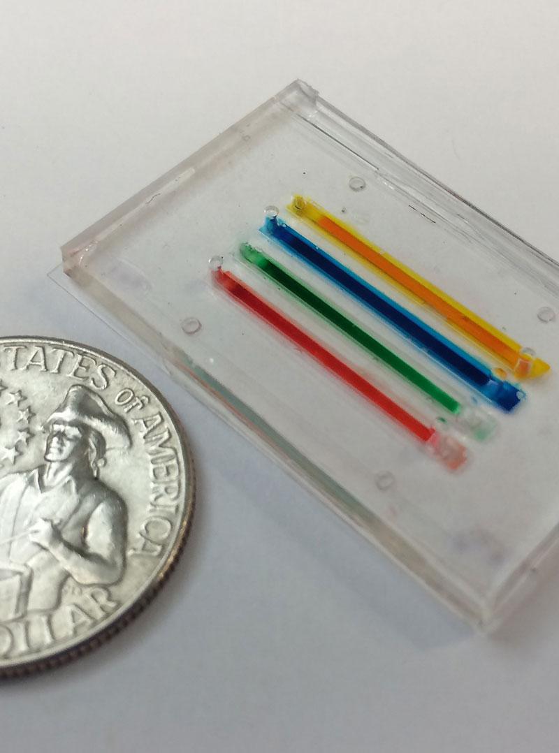
This microfluidic device is being used to study blood platelets to help doctors understand the complex blood clotting process. The research is being done in the laboratory of Dr. Wilbur Lam. (Photo: Lam Laboratory)
In one project, Lam and his research team are studying platelets, which are the tiny cell fragments responsible for blood clotting. With funding from the National Science Foundation (NSF), they’re looking at a basic question: How these 500-nanometer-thick cells actually stick together to seal up wounds, a process called platelet contraction.
Using a MEMS-based platform involving pairs of submicron- size protein dots to which platelets attach, the researchers have measured the force of platelet contraction. A better understanding of platelet behavior could help treat common diseases like stroke and heart attack that involve too much or too little clotting. In another project, Lam and his research team have developed an in vitro system that allows them to observe the three main elements of clotting — platelets, fibrin formation, and blood vessels — at the same time. The aim is to gain increased understanding of how the different components work together.
The researchers created a microfluidic device that replicates a blood vessel. They then grew a full endothelial cell layer that lines the entire inner surface of the device to create the artificial blood vessel. MEMS technology provided a trap-door structure that simulates a hole in the blood vessel to provide a model for bleeding.
MEMS AND THE INNER EAR
Health care applications such as implants can also take advantage of MEMS technologies. Pamela Bhatti, an associate professor in Georgia Tech’s School of Electrical and Computer Engineering, is studying the use of MEMS-based devices as a platform for treating problems in the inner ear. She’s looking specifically at cochlear implants that address hearing loss and vestibular prosthetic devices that treat loss of the sense of balance.
Implants into the cochlea, the auditory portion of the inner ear, have been used for years to address total hearing loss. Bhatti is investigating whether MEMS-based sensors could provide improved results when implanted in the cochlea.
One key issue involves the surgical challenge of handling a MEMS device that’s mounted on a polymer film substrate only 20 microns thick. The fragile device is difficult to place deep into the spiral-shaped cochlear cavity where it’s needed. Making the substrate thicker would help the device stand up to the force necessary for surgical placement, but would also make it larger and more difficult to fit into the tiny cochlear canal.
With NSF funding, Bhatti is studying a hybrid approach in which a MEMS-related device would be used in tandem with a hearing aid. The MEMS device could be implanted in the first turn of the cochlear spiral, which is easier to reach; there, it would detect the higher sound frequencies, while a more conventional hearing aid would pick up the lower tones.
One challenge is keeping the MEMS device thin enough to allow the cochlear fluid to conduct acoustic energy to the hearing aid.
“It’s a balancing act: You want the device to have small and precise features, and you also want it thick and malleable,” she said.
In research that involves a potential vestibular prosthetic device, Bhatti is working on a micron-size angular accelerometer that would replicate the motion-sensing capabilities of a gyroscope. The goal is to use electrode arrays to stimulate the human balance system and, thus, overcome loss due to damage to the vestibular area of the inner ear.
FLASHLIGHT INSIDE BLOOD VESSELS
Looking inside human coronary arteries can be facilitated by both the power and tiny profile of MEMS technology. Levent Degertekin, a professor in the George W. Woodruff School of Mechanical Engineering, is developing minute systems that can be mounted on a catheter used to find blockages in arteries.
Currently, physicians guide a catheter through the body’s arterial system by viewing it from outside using X-ray technology or magnetic resonance imaging (MRI), which are two-dimensional projections and provide limited resolution. Moreover, current catheters are equipped with 2-D ultrasound technology that doesn’t offer a frontal view.
Researchers led by Professor Levent Degertekin are developing a single-chip catheter-based MEMS device that would provide forward-looking, real-time, three-dimensional imaging from inside the heart, coronary arteries and peripheral blood vessels. (Photo: Rob Felt)
“Think of the current systems of moving the catheter as being like the GPS-based map in your car — it’s useful but it’s flat, and you can’t see that herd of sheep directly ahead of you,” Degertekin said. “The view from inside using today’s intravascular ultrasound doesn’t provide much help. It’s more like looking out a side window.”
Degertekin’s approach equips the catheter tip with a tiny MEMS device that uses 3-D ultrasound capable of showing what’s directly ahead in the artery. The work is sponsored by the National Institutes of Health.
He also wants to make these ultrasound systems compatible with MRI techniques instead of X-ray imaging. High-resolution 3-D MRI technology would give doctors a better outside view of the moving catheter, and avoid radiation-exposure issues.
“It’s a futuristic and challenging design. We’re basically jumping at least two steps ahead of current technology,” he said. “Combining 3-D ultrasound with MRI is challenging because the techniques can interfere with each other.”
Degertekin and his team are developing MEMS technology that produces 3-D ultrasound capabilities using thousands of tiny ceramic capacitors resembling drumheads. These tiny ultrasound elements, 30 microns wide, move up and down in response to acoustic signals. The drumheads are currently integrated with processing electronics on a single 1.4-millimeter silicon chip, and the researchers are working to reduce them to sub-millimeter size for some applications.
To support this tiny array, the team has also pioneered technology that reduces the number of cable connections to the catheter. This approach helps minimize catheter size.
NANOSCALE SENSING PARTS
Nanotubes and nanowires can be key to MEMS device functionality. These tiny features move in response to force or acceleration, generating electrical or other signals that convey important sensing information, or they may just increase the surface area of a sensing element.
Oliver Brand, IEN’s executive director and a professor in the School of Electrical and Computer Engineering, is developing a chemical sensor platform that uses tiny oscillating MEMS devices to sense volatile organic compounds (VOCs).
“These sensors work as miniature scales, weighing chemicals attached to them,” Brand said. Arrays of such MEMS sensors can be embedded in a small, low-power system that can detect toxic chemicals such as benzene in air and water samples.
In related research, Brand’s graduate students deposit arrays of nanowires on top of MEMS devices to increase the surface area to which a target chemical can attach. The result is improved sensor performance.
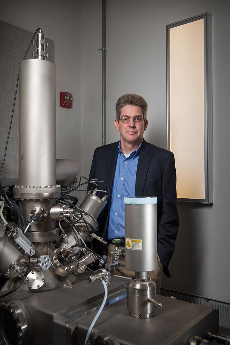
Professor Oliver Brand, director of the Institute for Electronics and Nanotechnology, is using tiny nanowires in MEMS devices to detect toxic chemicals such as benzene in air and water. In front of him is a ToF-SIMS system that can directly chemically image a surface.
DIAGNOSING DISEASE
Identifying harmful bacteria and viruses or other toxins in the environment is a task well suited to MEMS and other small-scale sensing technologies. Tiny sensors lend themselves to the development of portable devices that can provide real-time sensing useful in agriculture, food production, and similar settings.
Eric Vogel, a professor in Georgia Tech’s School of Materials Science and Engineering, researches two-dimensional materials, like graphene and molybdenum disulfide, that consist of single layers only one-atom thick. Such materials are being applied to multiple electronics uses, but they can also be used in microsystems for sensing applications.
This device is part of a system under development by Professor Eric Vogel and two Irish research teams that uses nanoscale thick 2-D materials, laminated onto plastic substrates, to produce disposable semiconductors for quickly diagnosing bovine respiratory disease.
Vogel and his team are collaborating with two Irish institutions — the Tyndall National Institute at University College Cork and Queens University, Belfast — to find improved methods for detecting bovine respiratory disease, a $2 billon problem worldwide. In a program jointly funded by the NSF, the Science Foundation Ireland, and Invest Northern Ireland, the three teams are developing a portable device to test for infection on site, eliminating the need to send blood samples to a lab.
“The problem is that the lab work takes a week or two, and by that point a sick cow could have infected 100 other cows,” Vogel said. “We’re developing a handheld device that could analyze special strips almost like a glucose sensor and would give rapid results at a low cost.”
To make these low-cost strips, Vogel and his team are using a technology called ion sensitive field effect transistors. Nanoscale-thick two-dimensional materials are laminated onto plastic substrates, producing disposable semiconductors at far less cost than conventional silicon.
These semiconductors will be coated with a chemical layer being developed at the University of Belfast. Target biological agents in a blood sample will bind to this chemical layer. Their specific electrical charge will then be detected by the semiconductor underneath, enabling a diagnosis on the spot.
FINDING FOODBORNE PATHOGENS
Food safety sensing can provide an important defense against foodborne illnesses, a major international health problem. Jie Xu, a senior research scientist at the Georgia Tech Research Institute (GTRI), is developing multiple microsystem-based technologies focused on detecting foodborne pathogens.
In one project, Xu is investigating the use of optical biosensors that use MEMS/microsystem technology to detect pathogens in real time. Using an IEN cleanroom, she has fabricated a prototype bio-detection device consisting of a microfabricated waveguide chip conjugated with bioreceptors specific to foodborne pathogens.
A top layer of bioreceptors provides a binding site that attracts specific target pathogens. The binding action produces a measureable change in the optical signal from the target molecule; the waveguide, constructed using a silicon nitride thin film, conducts this light signal to the charge-coupled device (CCD) microchip detector.
“You flow the sample, such as chicken rinse water, over the device, and if a pathogen such as Salmonella is present, it will bind to the bio-recognition element on the surface and give you a detectable signal,” Xu said.
EARLY WARNING OF CROP DISEASES
(Left to right) Milad Navaei, Jie Xu, and Peter Hesketh, photographed at the Atlanta Botanical Garden, are using MEMS-related technology to develop a portable gas chromatograph that could provide on-site, real-time detection of crop disease and alert farmers to the need for quick corrective action.
Identifying volatile organic compounds (VOCs) associated with crop disease can help farmers take quick action against pathogens. GTRI’s Jie Xu is working with Professor Peter Hesketh of the Georgia Tech School of Mechanical Engineering to develop another microsystem-based sensor platform, a portable gas chromatograph (GC) that detects VOCs in the air in real time.
The aim is to provide an early diagnostic capability that would let farmers take corrective action far sooner than traditional approaches that rely on visual inspection.
The researchers have fabricated a miniature GC that utilizes tiny separation columns micro-machined onto a silicon wafer. Combined with other sensors, it could seek a variety of fungus, mold, or other crop infections marked by the release of VOCs.
“We’re working toward a handheld GC that’s about cellphone size,” Hesketh said. “It would be a fraction of the size of traditional GCs, which use separation columns that are as long as 30 meters.”
Additional potential uses include mobile stations that track atmospheric pollution or those that monitor VOC emissions at locations associated with petroleum products, like oil refineries or power plants.
FINDING CONTAMINATION
Detecting microorganism contamination is another important element of Hesketh’s research. With funding from the U.S. Department of Agriculture, he’s working with a University of Georgia team on an improved method for detecting food contamination involving bacteria and viruses found in various sources.
The collaborators are developing a technique that uses magnetic beads to capture and extract microorganisms from a sample. The tiny beads are coated with an antibody that attracts the target organism.
The researchers place the sample and beads in a device that’s basically a compact disc etched with tiny microfluidic channels. The disc, rotating at extremely high speeds, is designed to mix the beads thoroughly with the sample, helping ensure that all the existing organisms are found.
To sense the extracted organisms, the researchers are designing a system that would use micro-cantilevers coated to attract the target bacteria. The cantilevers could employ tiny piezoelectric-resistive strain gauges capable of generating an electrical response when they make contact with the mass of even a single bacterium.
DETECTING DANGER
The sudden collapse of bridges and other structures in recent years has focused attention on aging U.S. infrastructure. Yang Wang, an associate professor in Georgia Tech’s School of Civil and Environmental Engineering, is collaborating with Professor Manos Tentzeris of the School of Electrical and Computer Engineering to develop devices that remotely monitor structures for stress and the formation of cracks.
These small strain sensors are low in cost, require no battery power, and can identify structural problems at an early stage. The research, which is also applicable to monitoring other structures beyond bridges, has been funded by the Federal Highway Administration and the Air Force Office of Scientific Research.
Associate Professor Yang Wang is collaborating with other Georgia Tech researchers on the use of microsystem technology to develop wireless strain sensors. Utilizing conductive silver nanoparticles printed on paper or polymer, they’re producing lowcost sensors to give early warning of stress-induced changes in bridges or other structures.
“This ‘smart-skin’ technology is completely wireless. It doesn’t need a battery, and you don’t have to climb around on structures running long connecting cables,” Wang said.
In this approach, small antennas tuned to specific radio frequencies are attached to various structural members. The antenna itself functions as the strain sensor. Even the slightest change in the structure deforms the antenna, producing an altered frequency response that can then be detected by a wireless reader.
Initially, the researchers developed a prototype strain/ crack sensor that was successfully tested in the laboratory. This prototype consisted of a small piece of copper deposited on a polymer substrate, along with a 1-millimeter-square radio frequency identification (RFID) chip. The copper antenna detected deformation, while the chip modulated the frequency response and functioned as a tag identifying the individual sensors.
Now more sophisticated designs are underway. Over the past few years, Wang’s and Tentzeris’ research groups have been developing wireless strain sensors that are made using conductive silver nanoparticles printed on paper or liquid crystal polymer. Aimed at low-cost mass production, the nanoparticle printing technique offers a promising replacement for traditional manufacturing of printed circuits with copper or other conductors.
Rick Robinson is a science and technology writer in Georgia Tech’s Institute Communications. He has been writing about defense, electronics, and other technology for more than 20 years.This story was originally published in the Georgia Tech Research Horizons magazine. Other stories from the magazine can be found at http://www.rh.gatech.edu/.


