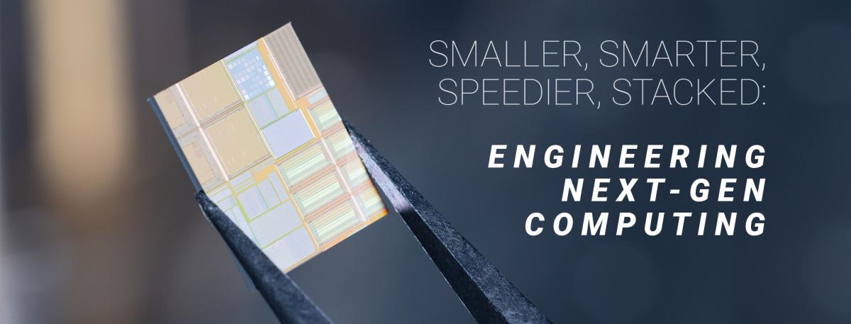
Some technologists suggest we’re nearing the limits of packing ever-more computing power into ever-smaller chips. At Georgia Tech, engineers are finding new ways to shrink transistors, make systems more efficient, and design better computers to power technologies not yet imagined.
(text and background only visible when logged in)
The power of modern computing is hard to overstate.
Your smartphone has more than 100,000 times the power of the computer that guided Apollo 11 to the moon. It’s about 5,000 times faster than 1980s supercomputers. And that’s just processing power.
Apple’s original iPod promised “1,000 songs in your pocket” in 2001. Today’s average smartphone has enough memory to store 25,000, along with thousands more photos, apps, and videos.
This exponential leap in capability traces a prediction made in 1965 by Intel co-founder Gordon Moore. He suggested the number of transistors — tiny electronic switches — on a computer chip would double roughly every two years. Moore’s Law, as it became known, has served as a benchmark and guiding principle for the tech industry, influencing the trajectory of innovation for nearly six decades.
But now miniaturizing transistors has slowed. Headlines regularly declare Moore’s Law dead.
Arijit Raychowdhury sees it differently.
He said Moore’s Law was never just about shrinking transistors. It was about making computing better.
“Moore’s Law is fundamentally economic,” said Raychowdhury, Steve W. Chaddick School Chair of Electrical and Computer Engineering (ECE). “It’s not about the physics of making transistors smaller. It’s about the business imperative to deliver better performance, lower power consumption, smaller form factors, or reduced costs.”
The current challenge, then, is not just putting more transistors on a chip; it’s engineering progress across what researchers call “the stack,” from the materials and devices at the bottom to the software at the top.
He pointed to NVIDIA’s latest Grace Blackwell chips announced in June. They deliver 30 times the performance of the previous generation while using half the energy. That, Raychowdhury said, is Moore’s Law in action — not just smaller transistors, but also system-level innovation.
The current challenge, then, is not just putting more transistors on a chip; it’s engineering progress across what researchers call “the stack,” from the materials and devices at the bottom to the software at the top.
The College of Engineering is driving this kind of innovation through major national initiatives accelerating computing hardware research, with Georgia Tech leading or directly involved in projects totaling more than $1 billion.
“It’s not just about advancing research,” Raychowdhury said. “We’re building the talent pipeline that’s vital to the future of the U.S. tech industry and national competitiveness.”
By driving breakthroughs across the computing stack and helping shape national strategy, Georgia Tech is carrying forward the spirit of Moore’s Law. The goal was never just smaller transistors. It was better computing. That vision is still alive — and still evolving — today.
(text and background only visible when logged in)
(text and background only visible when logged in)
The Foundation
Today’s computer engineering challenges still begin with transistors, the basic building blocks of computing. These tiny switches, now measured in nanometers, are the nucleus of every computational cell. Without them, there are no integrated circuits, no processors, no memory, and no compute systems.
Transistors are made from semiconductors, which are materials like silicon that can conduct electricity under certain conditions. Their ability to control and amplify electrical signals makes them ideal for building computational and storage systems that power everything from smartphones and laptops to supercomputers.
Engineers have worked for decades to make transistors smaller, fitting more of them on each chip and enabling faster, more efficient computing. Despite claims of Moore’s Law reaching its limits, this effort is far from over.
“The idea that transistor density scaling has stopped is a false narrative,” said Suman Datta, the Joseph M. Pettit Chair in Advanced Computing in ECE and a Georgia Research Alliance Eminent Scholar. “It’s just that the technology has become so advanced, only a few places are skilled enough to keep pushing the limits. But those that can, absolutely are.”
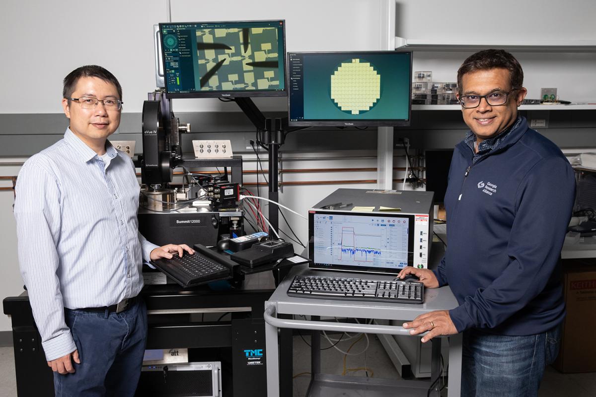
Shimeng Yu (left) and Suman Datta are building the next generation of computing hardware. Datta is building high-performance transistors at much lower temperatures, allowing them to be stacked vertically on a chip. Yu is reimagining computer memory design to improve performance.
The most advanced semiconductor technology can pack about 300 million transistors into a single square millimeter of silicon. For scale: a human hair could fit tens of thousands of modern transistors side by side across its width.
“We are literally dealing with atomic layers,” Datta said. “The gate dielectric [a tiny insulator in a semiconductor that helps switch electric signals] in some transistors is just 1.5 nanometers thick, which means only three or four layers of atoms.”
The newest smartphone chips have nearly 20 billion transistors. Taiwan Semiconductor Manufacturing Company, the world’s largest semiconductor foundry, has manufactured chips that contain around 100 billion transistors.
This level of precision requires new materials, new architectures, and new fabrication techniques. One of the most promising directions is vertical, or 3D, stacking, allowing chips to have more transistors without expanding the footprint.
But stacking transistors is not simple. The bottom layer of a chip is already optimized to the last atom and applying too much heat while building the top layers can damage what lies beneath.
(text and background only visible when logged in)
This level of precision requires new materials, new architectures, and new fabrication techniques. One of the most promising directions is vertical, or 3D, stacking, allowing chips to have more transistors without expanding the footprint.
(text and background only visible when logged in)
In Datta’s lab, the team is developing low-temperature fabrication methods that preserve reliability while enabling high-performance 3D integration.
“It’s not like sushi — you can’t serve it raw. You have to ‘cook’ the transistor to make it reliable,” he said. “But when you’re stacking layers, you can’t apply heat the way you normally would, or you’ll damage the layer underneath. We’re essentially building high-performance transistors in the cold.”
Advanced fabrication techniques like Datta’s that fabricate transistors in three dimensions are already showing up in test-chip designs in corporate research laboratories. And the need for such high-density chips is only accelerating.
“If you had asked me even five years ago, I might have said the semiconductor industry was heading for a slowdown,” he said. “Instead, the opposite happened. ChatGPT’s public launch in 2022 triggered a Cambrian explosion in semiconductors. Semiconductors have become the bottleneck and the backbone of the generative AI revolution. We must continue to stack transistors, use new materials, and push the limits of physics.”
(text and background only visible when logged in)
(text and background only visible when logged in)
Memory at the Center
With the rise of artificial intelligence, memory has become another major bottleneck. AI models contain trillions of parameters and rely on massive datasets. Every time a system processes information, it must retrieve it from memory, move it to the processor, and often send it back again. This constant movement burns energy and takes time.
“The future depends on high-performance memory. Without it, AI will consume all the energy in the world,” said Asif Khan, ON Semiconductor Professor in ECE.
In the 1970s, memory chips like Dynamic Random-Access Memory (DRAM), used for fast, temporary data storage, could only hold a few thousand bits of data. Today, the same type of chip can store billions. Solid-state drives using NAND flash memory, designed for long-term data storage that retains information even when the power is off, can hold several terabytes — enough to store hundreds of hours of video.
Each memory chip contains millions or billions of memory cells, the tiny circuits that store individual bits of data. But, like logic chips, progress has mostly come from shrinking components on a flat surface, an approach that is starting to hit physical limits.
Shimeng Yu’s lab is looking to improve memory performance at two levels: system-level integration and cell-level design.
At the system level, the team is changing how processors and memory chips are physically connected. Instead of placing them side by side, they’re stacked vertically, allowing data to move across the chips’ full surfaces rather than only a single narrow edge.
“We’re connecting across an entire plane,” said Yu, a Dean’s Professor in ECE. “That gives us more bandwidth and faster communication.”
This stacked design creates new thermal challenges, however. Heat trapped in the middle of the stack is harder to remove, so Yu’s lab is developing system design solutions that employ heat spreaders and conductive layers to manage energy and cooling.
At the cell level, Yu is rethinking the structure of DRAM itself. Traditional memory is built flat, but his lab is exploring 3D architectures that build upward, increasing density by stacking memory cells.
“Right now, we can fit about half a gigabit of data into the size of a grain of rice,” he said. “With 3D DRAM, we’re aiming to double or triple that, eventually reaching 10 times the current integration density.”
Yu is also exploring in-memory computing, where certain operations are performed directly within memory devices. This minimizes data movement, which is one of the largest sources of energy use in modern data centers.
“Every time you move data, you burn power,” Yu said. “We want to keep the data where it is and compute there.”
Khan is pushing even deeper into memory by focusing on the materials inside each cell. His lab is integrating ferroelectric materials to deliver DRAM-like speed with the persistent storage of flash memory.
“We’re trying to build memory that doesn’t just perform better, but operates on entirely new principles,” Khan said.
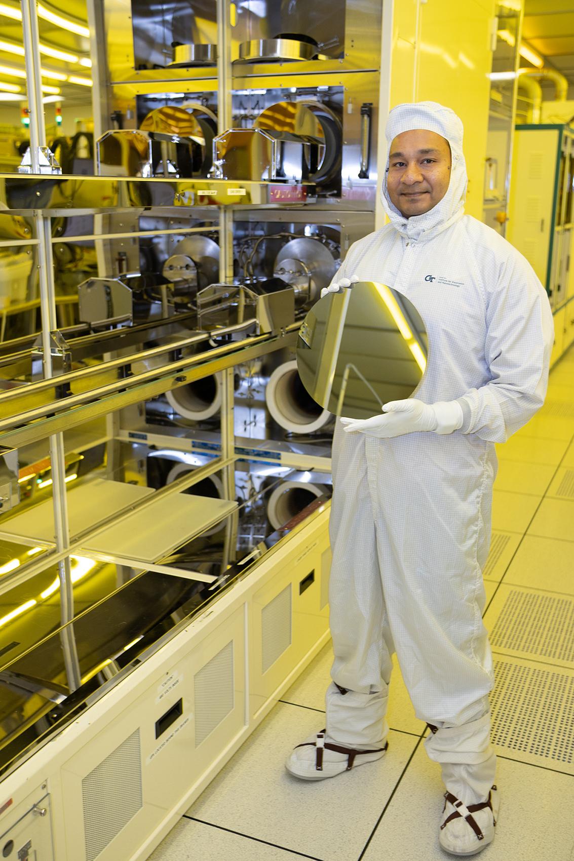
Asif Khan holds a silicon wafer in Georgia Tech’s cleanroom facility. Khan is trying to build new kinds of computer memory using fundamentally different mechanisms to store data.
Ferroelectric materials offer a fundamentally different mechanism for storing information. Instead of relying on the presence or absence of electrons, they use the orientation of electric dipoles — tiny shifts in atomic structure that can represent ones and zeros. This allows memory to retain information even when the power is turned off, while also using significantly less energy.
“Think of it like a spring,” Khan said. “In conventional memory, you must keep tension on the spring to hold its position using energy. In ferroelectric memory, the spring stays stretched. It remembers its state without needing extra energy.”
His group has demonstrated ferroelectric devices with promising scalability and endurance in the lab. They are collaborating with industry partners like Samsung and Micron to bring the technology closer to commercialization.
Both researchers emphasize that memory has become more than a supporting technology. It is a driving force behind the next wave of computing.
“We’re not just scaling devices,” Khan said. “We’re redefining what memory is and what it can do.”
(text and background only visible when logged in)
(text and background only visible when logged in)
The Rise of Advanced Packaging
As individual components reach physical limits, researchers also are considering how the components are arranged and connected using processes called advanced packaging. It’s an area where Georgia Tech has carved out a leadership role since the 1990s with the 3D Systems Packaging Research Center (3D-PRC).
“Packaging has become the new frontier. It’s where some of the most important innovations are happening,” said ECE Professor Muhannad Bakir, who directs the center. “The silicon world has been scaling for decades. Now packaging must scale just as fast.”
The reason is simple: Chips have become too large, too complex, and too expensive to manufacture as single units. Instead of building one massive chip, engineers now break it into smaller pieces called chiplets. When assembled into a complete system, they can outperform traditional monolithic designs.
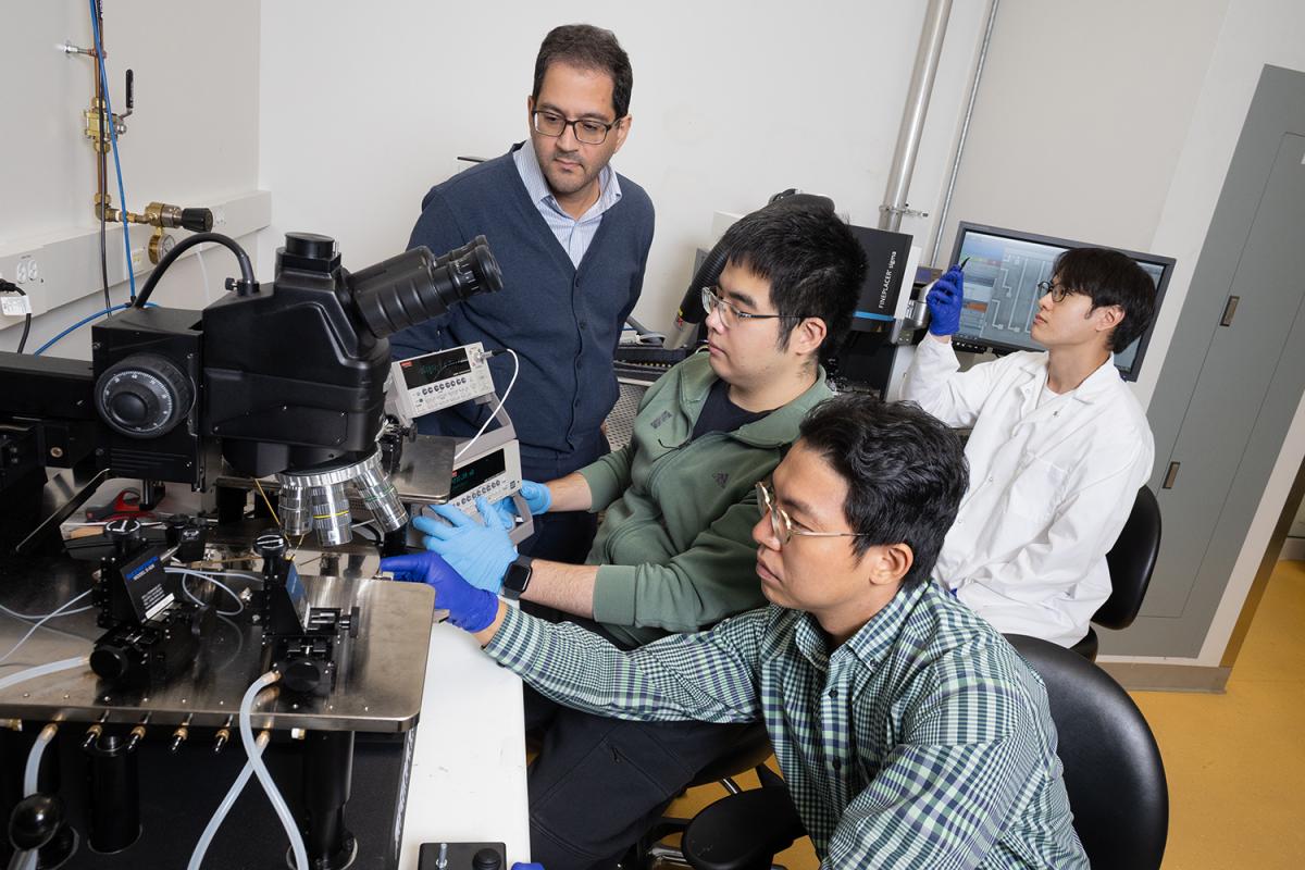
Muhannad Bakir (standing) leads Georgia Tech’s 3D Packaging Research Center, where researchers are developing new ways to arrange and connect the components on chips to increase performance.
“You can get increased functionality at lower cost and better performance,” Bakir said.
This strategy is part of a broader approach called heterogeneous packaging. It allows different parts of a system — logic, memory, power management, even photonics — to be built using the best available technologies and then tightly integrated.
“You’re not just gluing pieces together,” Bakir said. “You’re managing power delivery and dissipation, cooling, mechanical stress, signal integrity, data bandwidth, manufacturing constraints, and more all in a compact form factor. It’s a full-stack engineering challenge with so much room for innovation and impact.”
Georgia Tech’s research spans everything from 3D heterogeneous integration and chiplet architectures to glass-core substrates, a promising platform for large-scale AI computing systems.
Glass is flat, smooth, and mechanically stable, allowing for ultra-fine wiring and embedded components. It also can be made in much larger panels than silicon wafers, making it ideal for aggregating GPUs and memory modules in data centers.
“Glass allows you to actually embed electronics into the glass substrate,” Bakir said. “Typically, you glue things on top of the substrate. With glass, you can add functions into the core.”
Chips have become too large, too complex, and too expensive to manufacture as single units. Instead of building one massive chip, engineers now break it into smaller pieces called chiplets. When assembled into a complete system, they can outperform traditional monolithic designs.
Georgia Tech’s partnership with Absolics is accelerating this work. The manufacturer has built a $600 million facility in Covington, Georgia, to produce glass substrates. Absolics also has received $100 million to support a joint research program with Georgia Tech and other partners.
Georgia Tech’s leadership in semiconductor packaging builds on years of work.
Former Tech professor James Meindl helped define the limits of scaling and the importance of interconnects in computing systems. His work laid the foundation for many of today’s advanced packaging strategies. He also helped expand Georgia Tech’s cleanroom facilities, which are key for virtually all of the advanced packaging programs and research on campus.
Another Georgia Tech professor, Rao Tummala, was instrumental in establishing the 3D-PRC and advancing the concept of “system-on-package” — treating packaging not as an afterthought, but as a platform for integration, performance, and miniaturization.
(text and background only visible when logged in)
(text and background only visible when logged in)
The Communication Challenge
Modern computers move staggering volumes of data between processors, memory, and storage every second to keep up with the demands of AI, cloud computing, and real-time applications. The faster that data moves, the better systems perform.
But as workloads grow and architectures become more complex, traditional wiring is hitting its limits.
Ali Adibi is pioneering the use of light instead of electricity to transmit data within computing systems, with support from the Defense Advanced Research Projects Agency (DARPA).
“In computing, a major challenge is interconnection. You can build powerful processors, but they need to communicate with memory and other processors,” said Adibi, Joseph M. Pettit Faculty Chair in ECE. “That’s where optics becomes essential.”

Ali Adibi is pioneering the use of light instead of electricity to transmit data within computing systems. (Photo: Allison Carter)
The advantage lies in physics. Photons carry data in optical systems and operate at much higher frequencies than the electron-based signals in traditional systems. This allows them to transmit data considerably faster than electrons using conventional wires.
To harness that speed inside computing systems, Adibi’s team is designing 3D optical routing networks that guide light through tiny pathways built directly into the chip. These systems combine the essential parts of optical communication — like modulators, detectors, and waveguides — using fabrication techniques borrowed from the semiconductor industry. The result is a chip where optics and electronics work side by side.
Despite the promise of photonics, building these systems is far from simple. Integrating photonic elements with electronic systems demands precise alignment and consistent manufacturing.
“As with any complex system, success depends on how well everything is structured and optimized,” he said. “Once everything is in alignment, data can move faster, more efficiently, and with less energy consumption for communicating each bit of data.”
(text and background only visible when logged in)
(text and background only visible when logged in)
Avoiding Digital Gridlock
Moving data quickly only helps if the system can handle it. That’s where Tushar Krishna’s work begins.
The ECE associate professor focuses on the architecture and modeling of high-performance systems. His research helps engineers understand how to design computing platforms — from individual chips to large-scale clusters — that can handle modern workloads without getting bogged down.
“Efficient processing requires more than just powerful processors,” Krishna said. “It’s about how you move data, how you schedule tasks, and how you architect the system to minimize bottlenecks.”
His team tackles two key challenges. First, how to reuse data as much as possible to avoid unnecessary movement. Second, how to connect many processors so they can work together seamlessly.
“The problems we’re trying to solve are actually a little bit like designing road networks,” he said. “You have a lot of cars moving around, but finite roads. So, you need to answer questions like, ‘What’s the topology? Should I provide highways or small roads with traffic signals?’”
(text and background only visible when logged in)
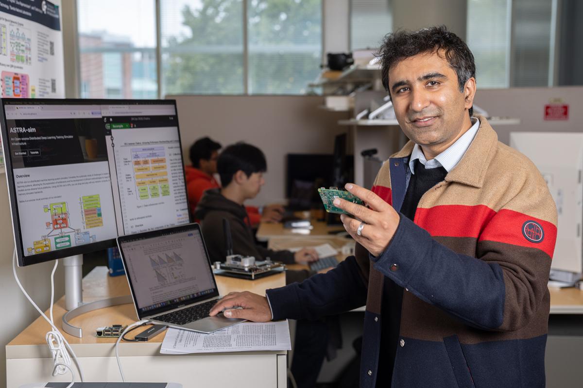
Tushar Krishna models high-performance computing platforms so engineers understand how to design them to handle modern workloads without creating data traffic jams.
Krishna’s lab builds simulation tools that model different system configurations before they are built. These tools allow researchers to explore trade-offs between performance, power, and flexibility.
In his analogy, cars are data and the roads are the communication pathways between processors. Krishna’s goal is to reduce data traffic jams by designing smarter, more efficient routes.
To help engineers make informed decisions, Krishna’s lab builds simulation tools that model different system configurations before they are built. These tools allow researchers to explore trade-offs between performance, power, and flexibility.
“We’ve created abstractions that help system designers understand what matters, like how many ‘cars’ are on the road and where they’re going, without needing to know the make and model of every vehicle,” Krishna said.
This approach allows engineers to focus on the flow of data without getting slowed down by the complexity of every individual computational task.
Krishna’s tools are open source, meaning they’re freely available to other researchers and companies. This has made it easier for others to test new ideas and simulate hypothetical hardware before investing in building it.
(text and background only visible when logged in)
Optimizing the Invisible Layer
Hardware provides the foundation, but software determines how that foundation is used.
This layer of the stack manages the flow of data and tasks across the computing system, making decisions that shape performance long before any application appears on screen for users. It includes things like operating systems, compilers that translate code into machine instructions, schedulers and workload managers, and more.
Today, most AI models can only run through the cloud on massive data centers. But by tightly integrating the design of algorithms, software, and hardware, researchers could make it possible for those same models to run efficiently on smaller servers, edge devices, or even smartphones.
To help enable that shift, Callie Hao is developing tools that bridge the gap between software and hardware, making AI systems more efficient, portable, and accessible.
“AI has become so resource-intensive that it’s inaccessible to many,” said Hao, Sutterfield Family Assistant Professor in ECE. “Computer engineers have a responsibility to make these technologies more efficient and available to everyone, not just a privileged few.”
Hao is exploring algorithm-accelerator co-design. Rather than designing hardware first and adapting AI models afterward, Hao works on them together, building tools that help AI programs use advanced chips more efficiently. One of these tools, called LightningSim, simulates — within milliseconds — the performance of complicated AI tasks running on customized accelerators. This makes it much easier to find an optimal design for the accelerator as well as the AI task mapping.
“With the right optimizations, we’re getting closer to executing these models on-device,” Hao said. “That’s a huge step toward making AI more practical and inclusive.”
Hao’s lab also is exploring how machine learning can assist in hardware design, creating a feedback loop where AI helps build better systems for AI.
“We need to use every tool at our disposal to engineer systems that are not just faster, but more adaptable and accessible,” she said. “The future is about delivering high performance computing wherever it’s needed, whether that’s in a data center or in your pocket.”
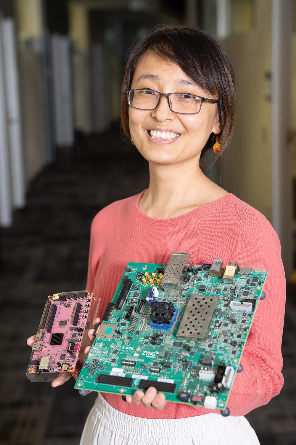
Callie Hao creates tools that help hardware and software work together so AI systems are more efficient, portable, and accessible.
(text and background only visible when logged in)
(text and background only visible when logged in)
Related Stories

Wearing the Future
From smart textiles to brain-computer links, Georgia Tech engineers are designing wearables that connect humans and machines more closely than ever to sense, respond, and heal.

Digital Doppelgängers
Engineers are building computerized replicas of cities, and even Georgia Tech’s campus, to save lives and create a better, more efficient world for all of us.

More Power, Less Heat
Alumnus and entrepreneur Edgar Garay is disrupting a $23 billion dollar industry with his reimagining of power amplifier chips.
(text and background only visible when logged in)
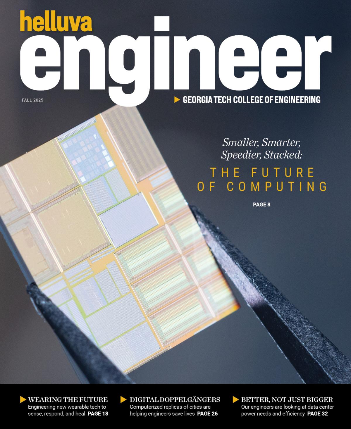
Helluva Engineer
This story originally appeared in the Fall 2025 issue of Helluva Engineer magazine.
The future of computing isn’t just about making chips smaller or faster; it’s about making computing better for people and society. And Georgia Tech engineers are shaping that future, designing the processors and memory that will power technologies we can’t yet imagine. They’re using today’s digital power to shape the physical world, helping people live healthier lives, making cities safer, and addressing the digital world’s huge demands on real-world land and resources. Smaller, smarter, faster — the pace of change in computing is accelerating; log into our latest issue to see how Georgia Tech engineers are making it all add up.